
NAND flash memory
What is NAND flash memory?
NAND flash memory is a type of non-volatile storage technology that does not require power to retain data. An important goal of NAND flash development has been to reduce the cost per bit and to increase maximum chip capacity so that flash memory can compete with magnetic storage devices, such as hard disks. NAND flash has found a market in devices to which large files are frequently uploaded and replaced. MP3 players, digital cameras and USB flash drives use NAND technology.
NAND flash saves data as blocks and relies on electric circuits to store data. When power is detached from NAND flash memory, a metal-oxide semiconductor will provide an extra charge to the memory cell, keeping the data. The metal-oxide semiconductor typically used is a floating-gate transistor (FGT). The FGTs are structured similar to NAND logic gates.
NAND memory cells are made with two types of gates, control and floating gates. Both gates will help control the flow of data. To program one cell, a voltage charge is sent to the control gate.
NAND flash memory operation
Flash memory is a special type of electronically erasable programmable read-only memory (EEPROM) chip. The flash circuit creates a grid of columns and rows. Each intersection of the grid holds two transistors separated by a thin oxide layer -- one transistor is called a floating gate and the other is called the control gate. The control gate connects the floating gate to its respective row in the grid.
As long as the control gate provides this link, the memory cell has a digital value of 1, which means the bit is erased. To change the cell to a digital value of 0 -- effectively to program the bit -- a process called Fowler-Nordheim tunneling, or simply tunneling, must take place.
Tunneling changes the way that electrons are placed in the floating gate. A signal voltage is sent along the respective column line of the grid, enters the floating gate and drains the charge on the floating gate to ground. This change causes electrons to be pushed across the oxide layer and alters the charge on the oxide layer, which creates a barrier between the floating and control gates. As this change drops the charge below a certain threshold voltage, the cell's value becomes a digital 0. A flash cell can be erased -- returned to digital 1 -- by applying a higher-voltage charge, which stops the tunneling and returns a charge to the floating gate.
This process requires voltage provided by active control circuitry. But the cells that compose the flash device will retain their charged or drained states indefinitely once external power to the chip is removed. This is what makes NAND flash memory non-volatile.
The process of charging and tunneling that takes place in a flash cell are destructive to the transistors, and the cell can only be programmed and erased a finite number of times before the cell starts to break down and fail. It's a flash concept called memory wear-out or just wear.
History and evolution of NAND flash memory
Flash memory traces its roots to the development of metal-oxide-semiconductor field-effect transistors (MOSFETs). MOSFET technology was developed in 1959, with the development of floating gate MOSFETs coming in 1967. Developers of these early transistors realized that the devices could hold states without external power and proposed their use as floating gate memory cells for programmable read-only memory (PROM) chips that would be both non-volatile and reprogrammable -- a potential boon in flexibility over existing ROM chips. These transistors formed the foundation of erasable PROM (EPROM) and EEPROM devices through the 1970s, though their use was limited.
Toshiba designers were the first to rearchitect groups of flash memory cells into blocks or groups and add the circuitry used to quickly erase entire blocks. This quick erasure was said to happen in a flash and the name stuck. NOR flash was proposed in 1984, and NAND flash was proposed in 1987.
Toshiba manufactured some of the first NAND flash devices in 1987, while Intel manufactured NOR flash devices in 1988. Removable memory card devices based on NAND, such as SmartMedia, appeared in the mid-1990s and involved several variations, including MultiMediaCard and other form factors. Removable cards, such as miniSD and microSD, evolved and provided better performance in smaller form factors.
Manufacturers made strides in NAND flash memory density, performance and reliability through the 2000s and 2010s, which took advantage of emerging cell design technologies such as multi-level cell (MLC) offering two bits per cell, triple-level cell (TLC) storing three bits per cell and quad-level cell (QLC) storing four bits per cell. Further advances in memory cell technology enable layers of memory cells to be stacked into layers to provide even greater flash storage capacity.
Types of NAND flash storage
Common types of NAND flash storage include SLC, MLC, TLC, QLC and 3D NAND. What separates each type is the number of bits per cell. The more bits stored in each cell, the less expensive the NAND flash storage would cost.
- SLC, or single-level cells, store one bit per cell. SLC has the highest endurance but is also the most expensive type of NAND flash storage.
- MLC, or multi-level cells, stores two bits per cell. Because erasures and write cycles occur two times more, MLC has less endurance compared to SLC. However, it's less expensive. Many PCs will use MLC.
- TLC, or triple-level cells, store three bits per cell. Many consumer-level products will use this because it is less expensive, however lower-performing.
- QLC, or quad-level cells, store four bits per cell. QLCs have even less endurance and are generally less expensive.
- 3D NAND -- 2D or planar NAND has only one layer of memory cells, whereas 3D NAND stacks cells on top of one another. Samsung refers to 3D NAND as Vertical NAND or V-NAND.
NAND flash shortage
The incessant demands of data storage and portable devices have spawned a shortage of NAND flash chips. The NAND flash shortage began in 2016 and has continued through 2021. The shortage is partially the result of demand, but it is also because vendors are transitioning from manufacturing 2D or planar NAND to much denser 3D NAND technology. Making 3D NAND chips is a more complicated process.
Today, solid-state drives (SSDs) and smartphones are primary drivers of the NAND flash market. The NAND flash memory market reached over $46 billion USD by 2020 and is expected to reach over $85 billion USD by 2026.
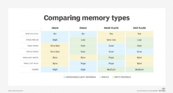
NAND flash vs. NOR flash
The two main kinds of flash are NAND and NOR flash memory, which get their names from their respective logic gates.
NAND flash memory is written and read in blocks that are smaller than the device, whereas NOR flash memory reads and writes bytes independently. Use cases for both NOR and NAND flash memory include laptop and desktop computers; digital cameras and audio players; smartphones; video games; and scientific, industrial and medical electronics.
NAND flash offers faster erase and write times than NOR flash, while NAND technology delivers better density at a lower cost per bit. NAND also offers up to 10 times the endurance of NOR.
NAND is not a suitable replacement for ROM because it does not deliver byte-level random access, which data stored on ROM usually requires. NOR memory makes a good replacement for RAM and ROM drives. NAND is more closely related to secondary storage devices, such as hard disks. This makes NAND flash good for mass storage use cases, such as SSDs.
Limitations and challenges of NAND flash memory
Flash memory technologies have provided enormous benefits to modern electronic devices -- from non-volatile memory cards in cameras to enterprise-class SSDs. But despite the benefits, flash technologies such as NAND flash memory present several key limitations and challenges that affect performance and reliability, including wear, erasure, crosstalk and sensitivity.
- Flash memory has a finite number of program/erase (P/E) cycles. Most basic flash products are rated for 100,000 P/E cycles before the storage cell integrity begins to fail, though some types of NAND flash chips are rated for 1 million P/E cycles or more. Wear is usually mitigated by spreading out write operations across the entire flash device, called wear leveling. Write verification and remapping techniques can also be employed to support bad block management. It's worth noting that read cycles aren't limited.
- Although flash memory can be written a byte or word at a time, flash memory must be erased in entire blocks. When a block is erased, all bits are set to 1. Once a bit is changed to 0, that entire block must be erased to change a bit back to 1. It takes finite time to erase a block before new writes can take place, limiting the overall performance of flash memory compared to other forms of volatile memory, such as dynamic RAM (DRAM). Erasure is also part of the memory wear issue.
- Reading NAND flash memory can cause nearby memory cells to change over time. It's a phenomenon called read disturb. In practical terms, it can take hundreds of thousands of reads to cause a bit change -- it's far more likely that the block will be erased and reprogrammed well before the read disturb threshold is reached. However, flash circuitry can count read cycles and intervene to copy the block before a read disturb event can occur.
- High-energy particles, such as X-rays, can sometimes change 0s into 1s in an array of flash memory cells. X-ray resistant memory devices are available to help prevent such issues.
NAND flash memory industry and vendors
According to Mordor Intelligence, the NAND flash memory market was estimated worth over 46 billion USD in 2020, and it's forecast to exceed 85 billion USD by 2026 -- a CAGR of 11.27%. This growth is expected to be driven by demand from computer devices such as smartphones, memory cards, SSDs and even memory-intensive projects such as artificial intelligence. There are six principal global manufacturers of NAND flash memory devices including:
- Samsung Electronics
- Kioxia
- Western Digital (WD) Corporation
- Micron Technology
- SK Hynix
- Intel
Future of NAND flash memory
NAND flash memory has become a vital component of modern mobile electronic devices. As these devices proliferate and strive to offer more features and functions, ever-larger volumes of NAND flash memory will be demanded to handle the growing code and data storage needs.
The primary goal of NAND flash memory design and evolution is density -- packing more bits into smaller and lower-profile chips. Recent years have seen the development of 128-layer 4D NAND from SK Hynix. This effectively enables the production of practical 1 TB NAND storage devices with chip package thickness of just 1 mm -- ideal for smartphones. Similarly, Samsung has produced a V-NAND device with over 100 layers offering better memory performance from lower latency and lower power consumption.
These fundamental drives toward greater capacity and superior performance will likely shape the future of NAND devices. Manufacturers are already developing 192-layer 3D NAND and 256-layer NAND devices are coming down the line. Manufacturers will meet these goals through the use of innovative flash circuit designs along with ever-improving semiconductor materials and fabrication technologies that produce flash wafers. Simultaneously, flash manufacturers will seek to improve the reliability of NAND devices into the future by extending their wear life and reducing the potential for bit error -- such as read disturb -- phenomenon.