
3D NAND flash
What is 3D NAND flash?
3D NAND is a type of non-volatile flash memory in which the memory cells are stacked vertically in multiple layers. The design and fabrication of 3D NAND memory is radically different than traditional 2D -- or planar -- NAND in which the memory cells are arranged in a simple two-dimensional matrix.
2D and 3D NAND basics
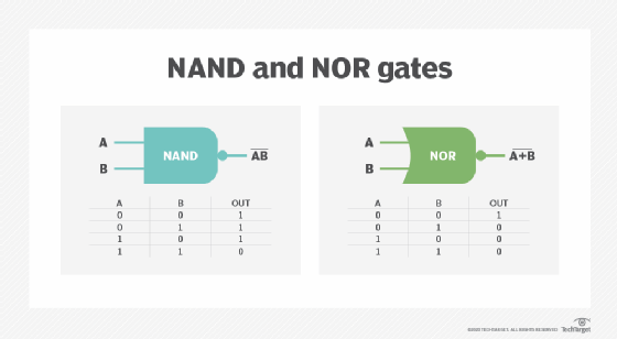
A flash memory cell is fundamentally a standard, low-power logic gate, and all logic gates use a well-understood binary input/output (I/O) relationship. The table that lists the relationship of logic gate input and output is called a truth table.
When Toshiba originally developed flash memory back in the 1980s, the memory devices were based on two distinctly different types of logic gates: NOR, which stands for NOT-OR, and NAND, which stands for NOT-AND. Both designs store data in memory cells built with floating gate transistors (FGTs).
Today, NAND flash technology has emerged as the most popular and widely used type of flash memory cell. Figure 1 shows basic NAND and NOR gates for students of basic digital electronics.
Flash memory gained popularity due to its non-volatile nature. That is, each memory cell can retain its binary state, a logical zero or one -- the data -- without the need for continuous power. This is dramatically different than dynamic RAM (DRAM), where every memory cell must be continuously refreshed to retain its binary state. Non-volatile rewritable memory has provided convenient, portable memory devices for a wide range of devices, such as imaging and video recording devices, thumb drives for storing and transferring files and data, and practical solid-state drive (SSD) devices as practical alternatives to traditional magnetic rotating media, such as hard disk drives (HDDs).
As with DRAM, 2D flash devices are designed and fabricated with memory cells arranged in a horizontal 2D matrix. This well-proven approach poses capacity and performance challenges because of limited space on the silicon die -- the chip itself. To increase storage capacity, the resulting memory cells must either be smaller, the die larger or both. Because memory cell fabrication can't get much smaller within the limits of today's fabrication technology, the resulting 2D flash device must get larger, presenting longer connections between memory cells that add latency and diminish performance. Thus, 2D flash components, or chips, are currently limited to capacities of 128 gigabytes (GB). In actual practice, a storage device can contain numerous chips to provide much greater capacity.
3D flash devices boost capacity and performance by stacking memory cells into vertical layers rather than a single horizontal layer. This effectively multiplies the available memory cells for a given area, enabling far greater storage capacities while using a smaller footprint. In addition, the stacking enables shorter overall connections for each memory cell, which supports faster memory performance. 3D flash is a relatively new fabrication approach, but capacities of 256 GB and 512 GB are available with the potential for far larger memory devices. Some of the newest 3D flash memory components tout 1 terabyte (TB) of capacity.
How do flash and 3D NAND work?
Flash memory is an advanced type of electrically erasable programmable read-only memory (EEPROM) -- the kind of non-volatile memory that traditionally holds firmware such as the BIOS in a PC. Flash memory stores data in arrays of transistors, which can be designed to store one, two, three or four data bits. The metal-oxide semiconductor-based FGTs used to fabricate the memory cells employ two gates instead of one. One gate is a floating gate, and the other gate is a control gate. In effect, the series of gates acts as a switch where the control gate captures electrons and moves them to the control gate. This kind of architecture enables the transistor to preserve the state of each memory cell when electrical power is removed.
As with older and more traditional EEPROMs, a flash memory cell must be erased before it can be rewritten. An EEPROM erases data byte by byte. In a flash memory device, tunneling electrons clear any charge on the FGT in a flash -- thus, the name flash memory -- enabling contents to be rewritten.
NOR flash is architected to provide high-speed access to individual memory locations, making NOR well suited for tasks that depend on optimum speed and access, such as modern PC firmware, effectively making older EEPROM-type devices obsolete. By comparison, NAND flash is designed to work with blocks of data called pages. This makes NAND flash well suited for high-speed sequential reads/writes for high-volume data activities, such as video and images. NAND provides fast read operation and is less expensive than NOR. Consequently, NAND flash is the predominant flash memory technology for many consumer and industrial devices.
Unlike DRAM, all-flash memory offers a finite number of program/erase cycles (P/E cycles) -- a characteristic referred to as endurance. The behavior of tunneling electrons used to erase the memory cell eventually causes the memory cell to wear out and fail. As this happens, the fault management capabilities of the flash memory device work to relocate bad cells and bad blocks, resulting in more time needed to write, or program, which slows the flash memory performance. Fortunately, the endurance of most modern flash memory devices is many thousands of P/E cycles. And this life is extended by wear-leveling techniques, which ensure that all of the memory is written before cells are erased, basically preventing the same subsets of memory cells from being erased and rewritten frequently, while other areas of the chip are left relatively unused.
To better understand wear leveling, consider a series of four containers labeled A, B, C and D, which represent pages of flash memory. Suppose that an object representing a page of data is placed in container A. That object is removed and changed, but rather than place it directly back into container A, it's placed instead into container B. When that object is next removed and changed, it's placed into container C and so on until the object is manipulated and finally placed into container D. Only then, when the object is removed and changed once again, is it placed back into container A. This basic wear-leveling concept enables flash memory to dramatically extend its working life.
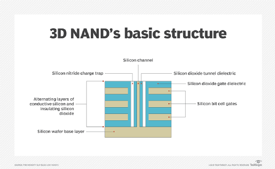
To make the move from 2D flash to 3D flash, the fabrication process adds multiple layers of memory cells on top of each other, along with interconnections between the layers. A typical 3D NAND flash chip can easily involve 32 to 128 layers, and even 256-layer devices are coming. The addition of layers makes 3D flash more difficult and time-consuming to fabricate than 2D flash. However, layers enable far greater bit densities within the memory device with far shorter connection paths, which brings better memory performance.
Today, 3D NAND flash devices are common in computers, such as tablets, as well as storage devices, such as flash memory cards, USB thumb drives, flash arrays and enterprise-grade SSDs.
Pros and cons of 3D NAND vs. 2D NAND
Both 3D and 2D NAND flash memory devices are readily available and in use today. But there are tradeoffs to consider when selecting the best technology for a storage task.
Capacity
3D NAND flash offers greater storage capacity -- or data density -- compared to 2D NAND flash. Stacking multiple layers of memory cells to create a 3D storage matrix can bring significantly greater storage capacity to the same chip area or footprint. Similarly, denser chips can be built into higher-capacity devices, such as SSDs. For example, SSDs are readily available in 1 TB and 2 TB capacities.
Cost
Flash memory follows the same cost-per-byte relationship as other storage technologies, and 3D NAND flash can vastly lower the cost per byte when compared to 2D NAND flash. Every layer added to a 3D NAND memory chip multiplies its capacity. Even if the 3D NAND wafer is several times more expensive to manufacture than a 2D NAND wafer, the dramatic capacity improvement of the 3D wafer makes the cost per byte far lower for the 3D NAND technology. This makes 3D NAND more cost-effective for many types of storage applications.
Performance and power
When memory cells are laid out in a 2D matrix, there's a finite distance to move bits to and from cells. This distance equates to time -- or latency. To increase the storage capacity of the 2D matrix, those distances -- and the latency -- must also increase, effectively lowering the performance of larger or higher-capacity 2D NAND flash devices. By stacking and interconnecting layers of NAND memory cells, the physical distance -- and, thus, the latency -- can be curtailed to maintain higher performance at higher storage capacities. In addition, 3D NAND flash memory can be written in a single pass and uses up to 50% less power than 2D NAND.
Manufacturing challenges
3D NAND flash devices can be extremely difficult to fabricate, requiring thousands of individual processes to take a raw wafer through to completed dies, or chips. Errors or contamination at any part of the fabrication process can introduce bad cells and render entire dies unusable. Good manufacturing demands extraordinary precautions against contamination, extremely high manufacturing control and material purity. Fortunately, such complex chip fabrication technologies are now mature and reliable to produce good yields for 3D NAND chip manufacturers.
Complex flash control
Although flash memory technology doesn't require refresh circuitry as with DRAM, it does require sophisticated data management, wear leveling and error correction control to oversee the way that data is stored on a flash chip. For example, 3D NAND flash might need to remap or move an entire block or page of storage if even a single bit fails, so additional control circuitry is needed to check for bit failures. At the same time, additional control is needed for wear leveling, spreading out the data stored throughout the chip to minimize P/E cycles and extending the flash device's working life. These controls are more complex for 3D NAND versus 2D NAND.
NAND types
NAND technology can be broken down into several specific designs, including single-level cell (SLC), multi-level cell (MLC), triple-level cell (TLC), quad-level cell (QLC) and even penta-level cell (PLC). The specific design typically relates to the number of bits held in each NAND memory cell, as well as characteristics such as endurance. 3D NAND flash devices can typically employ MLC, TLC, QLC and PLC designs but not SLC.
SLC
This NAND design stores 1 bit per memory cell. Because only one cell is involved in each P/E cycle, the cells are erased and rewritten least frequently on average, leading to some of the best endurance for NAND memory. A typical SLC device can be erased and rewritten about 60,000 to 100,000 times. In addition, the failure of a memory cell only affects that corresponding bit, making failures easier to remap and contain within the flash chip. Unfortunately, SLC is also the most expensive type of NAND flash in terms of cost per bit and is often reserved for the highest-performance mission-critical enterprise tasks, such as database applications.
MLC
This design stores 2 bits per memory cell. This improves the capacity of the flash memory device and lowers the cost because there are twice as many bits per cell compared to SLC. But endurance is affected because 2 bits must be erased and rewritten when the cell is rewritten, so the cell wears out faster. An MLC device can be erased and rewritten between 1,500 and 3,000 times. Performance and endurance are still attractive for most general-purpose applications with modest I/O needs, and MLC is frequently used in everyday computing devices, such as laptops. 3D NAND can employ MLC flash. Enterprise MLC is a variation of MLC that provides enhanced wear leveling control, which improves overall endurance and makes the device better suited to enterprise environments.
TLC
This type of NAND stores 3 bits per memory cell. This continued the push toward added flash capacity and lower costs. But the additional bit lowers performance slightly, and the P/E cycle now affects 3 bits instead of one or two, lowering the device endurance even further. TLC is more frequently employed for read-heavy tasks where P/E cycles are less frequent, helping to maximize endurance and preserve the working life of the TLC device. 3D NAND can employ TLC flash, and a typical 3D TLC device can be rewritten anywhere from 500 to 1,000 times.
QLC
This design stores 4 bits per memory cell. This technology represents some of the highest capacity and lowest cost of all NAND types, but it also poses lower memory cell endurance and performance compared to other flash technology. Advanced error correction and wear leveling controllers help to extend QLC device endurance, and the technology can prove attractive for read-heavy tasks where rewrites are infrequent, such as archival storage. A typical QLC cell can be rewritten about 100 times, though wear leveling can improve this to about 1,000 times. 3D NAND can employ QLC flash.
PLC
This is a relatively new type of NAND flash introduced in prototype SSDs in 2022, with practical devices expected in the market around 2025. It can store 5 bits per memory cell. PLC technology offers even better cost/density capabilities than prior NAND types but poses far greater complexity in storage, making each cell extremely sensitive to wear. Current PLC NAND devices list P/E endurance in terms of single digits. Low endurance likely demands extensive wear management controls and limits PLC-based devices to read-heavy applications for the foreseeable future.
3D NAND use cases
Flash memory is attractive in a broad range of use cases where mobility, non-volatility and physical resilience, such as shock, pressure and temperature, are useful attributes. The following examples offer a cross section of common use cases.
USB thumb drives
First introduced around 2002, USB drives provide small, portable, non-volatile storage options for all types of individual and small business computer users. In effect, the USB drive is a self-contained storage subsystem, including both the high-performance memory capacity along with all controlling circuitry. Today's USB drives range from simple 8-16 GB devices up to 1 TB. Some high-end USB drives even include features such as encryption and password security.
Flash memory cards
First appearing in the mid-1990s, flash memory cards have evolved to offer plugin convenience for many types of electronic devices, including cameras, tablets and video recorders, such as GoPro cameras. Today's flash memory cards can provide as much as 512 GB of storage capacity, with common data transfer rates ranging from 80 MB per second to 170 MBps. Flash memory cards are available in numerous form factors, including Secure Digital, microSD, miniSD and CompactFlash. Each form factor provides shapes and sizes tailored to different target devices, such as cameras and video recorders.
SSDs
SSDs appear in devices ranging from laptops to enterprise-grade storage arrays. They can replace traditional magnetic hard drives, bringing extremely fast I/O operations per second and lower power consumption to computing systems, while the removal of any moving parts improves drive reliability and reduces noise. Today's SSD products are readily available from 120 GB and upward into the 4 TB range and easily rival the high capacities and competitive price points typically associated with HDDs. SSDs are often used in flash storage arrays and other computing deployments, such as hyper-converged infrastructure products. SSDs are available to meet standard computer interface designs, including Serial Advanced Technology Attachment, or SATA; non-volatile memory express, or NVMe; and machine-to-machine Peripheral Component Interconnect Express, or M2M PCIe, enabling the device to be added to a computer in several possible ways.
3D NAND vendors
There are few 3D NAND flash memory manufacturers. This is due to the enormous capital investment required for flash chip fabrication in highly sophisticated manufacturing facilities called fabs, as well as the significant and specialized intellectual property involved, such as patents surrounding the technology. Today, there are five major manufacturers of 3D NAND flash devices:
- Kioxia, spun off from Toshiba.
- Micron Technology using the Crucial brand.
- Samsung, the original 3D NAND manufacturer.
- SK Hynix using the Klevv brand and now controlling Intel flash market share.
- Western Digital using the SanDisk brand.
The future of 3D NAND
3D NAND flash technology continues to push the limits of chip manufacturing capability. Although there are no significant new flash technologies poised to replace 3D NAND flash, manufacturers face enormous challenges building on the technology into the future. Rather than alternative storage technologies, 3D NAND is expected to address more fundamental issues, including the following:
- Capacity. Flash manufacturers seek to fit more bits of storage onto the same chip die. This typically involves more layers. Whereas chips will soon include up to 256 NAND flash layers, future 3D NAND chips will strive to push past this and include even more layers, stretching the limits of chip fabrication. Some manufacturers might opt for techniques such as string stacking, where larger chips are built from two or more smaller chips, e.g., stacking two 128-layer 3D NAND flash chips to create one 256-layer 3D NAND flash device. Other possible techniques include trenching, where the physical formation of the chip layers enables more cells to be packed closer together, further increasing cell density.
- Bit efficiency. The promise of PLC NAND flash to store 5 bits per cell is enticing, but it requires evermore complex and sensitive circuitry to write and read the bit patterns in each cell. This also pushes the current limits of chip design and manufacturing, but it's a viable pathway to more capacity per chip.
- Endurance. Complex 3D NAND chips are significantly more sensitive and able to tolerate far fewer erase/write cycles before NAND cells start to wear out and fail. Whereas the latest QLC and PLC chips offer relatively low endurance, NAND flash manufacturers are looking for ways to improve effective endurance through better materials, processes and supporting flash management circuitry, such as wear leveling and other techniques. Better endurance translates into more use cases and broader adoption of flash storage for a wider range of applications.
Before choosing between NAND or NOR flash memory, it's important to examine the structural differences between the two types of non-volatile memory.