Part of:Google Cloud Next 2026 conference coverage
New Google TPUs multiply AI infrastructure efficiency
Google's new TPUs assault AI's 'memory wall,' slash AI inference latency and lower costs, setting up its enterprise cloud services to compete on price and power efficiency.
LAS VEGAS -- A Google TPU refresh unveiled this week lays the groundwork for more cost and power efficiency in the cloud provider's AI infrastructure.
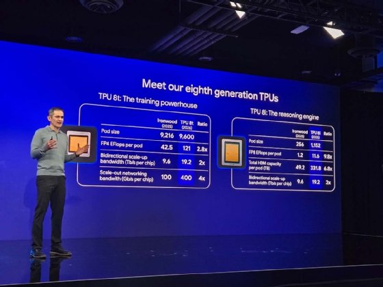
Google introduced two separate Tensor Processing Unit (TPUs) chips in its eighth-generation refresh, the first time it has split the product line since its launch in 2015. The TPU 8t is designed for AI model training, with 9,600 chips per pod and twice the memory bandwidth and four times the networking bandwidth per chip compared to the previous generation of TPUs. The Google TPU 8t also packs in 2 PB of shared high-bandwidth memory per pod.
In addition to computational power, the TPU 8t is designed with better reliability in mind, said Amin Vahdat, senior vice president and chief technologist for AI and infrastructure at Google.
"When we talk about our systems … it's not just 9,600 chips that are working on a problem. In many cases, it's tens of thousands, and, dare I say, more, that are all coordinating together at literally nanosecond scale," Vahdat said during a media event here at the Google Cloud Next conference this week. "What this means is that if any one chip fails, computation stops."
The new TPU 8t system targets not just high throughput but more than 97% consistent “goodput” -- a measure of useful, productive compute time. This was achieved with improvements to the way the system performs automatic detection and rerouting around faulty Inter-Chip Interconnect (ICI) links without interrupting a job and reconfigures hardware around failures with no human intervention.
The TPU 8i is designed to support AI inference, with a new custom ICI layer called Boardfly that breaks AI's "memory wall," a longstanding problem in AI infrastructure in which computational demands outpace the speed and capacity of chip memory. The new ICI for the TPU 8i doubles the previous generation's memory bandwidth and reduces the distance between chips in a pod, enabling them to work as a cohesive unit with the low latency required for mixture of experts models used for inference.
"Our default way of connecting [chips] together didn't support latency; it supported throughput, it supported bandwidth," in previous generations of TPUs, Vahdat said. "It was really good at getting large amounts of data through. But what you really care about in the age of agents, is the latency, the minimum time it takes to get the data."
Breaking the "memory wall" marks a potentially significant competitive shift for Google in AI chips, said Larry Carvalho, principal consultant at RobustCloud.
"There is a shortage of memory, and any vendor that optimizes memory can deliver AI at scale without having to deal with supply chain issues," Carvalho said. "With more AI compute going towards inferencing, this could be a big differentiator for Google."
Amin Vahdat, Google's senior vice president and chief technologist for AI and infrastructure, presents the eighth generation of TPUs at Google Cloud Next 2026.
Nvidia GPUs vs. Google TPUs
Google officials were using many of the same terms to describe this week's TPU updates, including optimization for inference separately from model training, that Nvidia used when it launched its Vera Rubin system for AI inference in January, but the two systems are designed for different forms of performance optimization, said Chirag Dekate, an analyst at Gartner.
"They are actually operating in two different trade-off spaces," Dekate said. "What Nvidia is designing for is being able to engineer something that can be deployed in broader domains, in broader ecosystems such as neoclouds and hyperscalers. Google's TPUs are designed [to be] predominantly managed and served by Google or experts who understand the TPU architecture."
While Nvidia must balance its general-purpose GPU and CPU systems to accommodate a broad set of potential workloads, Google TPUs, which started as application-specific integrated circuits (ASICs), are much more specialized for the specific computations performed during AI training and inference, according to Dekate.
"Nvidia GTC was laser-focused on creating token factories, not necessarily AI factories," he said. "ASICs will always [perform] better than any general-purpose architecture. That's the reality."
Specifically, "Nvidia follows a scale-up philosophy with its NVLink 6, engineered for maximum flexibility and ultra-low latency within a single rack environment," said Ron Westfall, an analyst at HyperFrame Research. "While multiple racks can link through InfiniBand to achieve petabyte-level aggregate memory, that data must traverse traditional networking protocols, introducing unavoidable latency.
The market conversation is going to shift from the volume of tokens that you're generating to the utility of tokens and intelligence per dollar.
Chirag Dekate, Analyst, Gartner
"In contrast, Google’s single machine philosophy enables 9,600 TPUs to function as a unified entity within a single global address space," Westfall said. "Because this interconnect integrates directly into the silicon, Google can pool 2 PB of memory into a single superpod, bypassing the performance bottlenecks typically associated with standard data center networking [and] operating with a level of cohesion that traditional clusters cannot match."
The upshot for enterprise IT buyers? Since most will access AI chips through cloud providers rather than running them in-house, new Google TPUs will set its AI infrastructure services up for greatly improved power and cost efficiency, Dekate said.
"Especially in the US and Europe, we are energy-constrained," he said. "The market conversation is going to shift from the volume of tokens that you're generating to the utility of tokens and intelligence per dollar, intelligence per watt. So it's actually power efficiency and cost efficiency and value that you generate per token that matters a lot more."
Still, Google isn't the only vendor heating up competition in AI chips -- AWS this week also announced a 5 gigawatt data center deal with Anthropic to train and deploy its Claude models on its AWS Trainium chips.
"Google TPUs are mostly for Google use, with some usage by Anthropic," Carvalho said. "On the other hand, Amazon Trainium is powering Anthropic workloads with an entire data center built on it. This is a win-win for both Amazon and Anthropic."
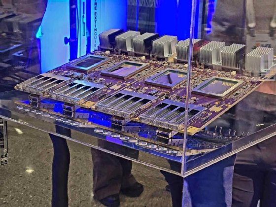
Google's TPU 8i system, on display at a press event during Google Cloud Next 2026.
Google exec predicts CPU comeback
Google Cloud also pledged this week to support Nvidia Vera Rubin systems alongside its TPUs and added support for its own latest Axion custom Arm CPUs, launched in January, which it claims delivers 100% better price-performance than general-purpose x86 CPUs. The TPU 8i system will also support Axion CPUs.
"There's a lot of general-purpose compute that is involved in running AI agents," Vahdat said. "They're creating sandboxes, virtual machines to build code, run it, check the results and then find the next set of outputs. So, general-purpose compute is going to make a comeback."
At the same time, what Vahdat termed the "age of specialization" will also continue in AI infrastructure.
"We're going to find additional workloads that might need their own chip," he said. "At a time when general-purpose CPUs are really only improving performance 5% a year, you have to specialize if you're going to go after brand new workloads. So two chips might become more."
Beth Pariseau, senior news writer for Informa TechTarget, is an award-winning veteran of IT journalism. Have a tip? Email her or connect on LinkedIn.