Flash memory guide to architecture, types and products
Flash memory, a staple of consumer electronics, is playing a wider role in enterprise storage. This guide offers an overview of flash, from current use cases to future directions.
Flash memory, also known as flash storage or simply flash, demands a closer look.
Flash technology permeates a multitude of consumer products, from mobile phones to ubiquitous USB memory cards. Enterprise flash, meanwhile, plays an expanding role in data center storage, server and networking technologies. Flash, despite its name, isn't the most visible of technologies -- it's typically embedded in other products -- but flash memory is everywhere.
This flash memory guide covers uses for flash memory, the technology's history and its advantages and drawbacks. The guide also provides an overview of the different flavors of flash, from single-level cell chips to 3D NAND. We'll also look at the current tradeoffs and the foreseeable future of this far-reaching electronic component technology.
What is flash memory used for?
Flash memory is widely used for storage and data transfer. In the consumer sector, flash memory finds a home in a range of devices, including phones, cameras and tablets, to name a few examples. Flash memory's small size and power consumption advantages make it well suited for use in on-the-go consumer devices. Indeed, consumer applications have helped propel the growth of the flash technology market.
Flash storage, a term often used interchangeably with flash memory, refers to any drive, repository or system using flash memory. At the consumer level, storage devices using flash include USB drives -- often referred to as thumb drives. In computer systems, flash-based SSDs, so called for their lack of moving parts, are prevalent in notebook computers and can also be found in many desktop PCs as a hard drive option.
SSDs have also established themselves in the data center in recent years. Here, flash storage adoption continues to expand in the form of enterprise-class all-flash SSDs, storage caches and storage arrays. Early flash storage deployments focused on caches for accelerating I/O-intensive applications, which remain popular candidates for flash storage.
Declining costs and increasing density have enabled organizations to extend their use of flash storage from specialized uses to general enterprise workloads. Lower prices put data centers in a better position to buy flash in anticipation of future needs.
Flash SSDs can be an attractive choice for read-intensive and low-latency workloads, but traditional magnetic HDDs remain popular for other key uses, such as long-term data storage, backups, archives and many noncritical enterprise workloads.
Flash and the digital enterprise
The rise of digital businesses also has contributed to flash storage adoption. In such enterprises, machine learning workloads and high-level analytics are among the developments requiring faster data access. Almost any read-heavy workload -- even database applications, such as SQL -- can use flash storage to accelerate response times, speed data processing and improve user experience.
Also, the price of flash has come down, making the storage technology feasible for a higher percentage of workloads in a higher percentage of companies, including digital businesses that were already inclined to invest in flash storage.
Matching the capabilities of the technology to workload needs and expectations seems to be the greatest flash issue for today's enterprises. Organizations will typically embrace flash for some workloads while relying on traditional HDD storage systems for others. The result is often the establishment of a storage tiering initiative that deploys several storage systems or types within the infrastructure:
- Tier 1. The highest tier is used for mission-critical workloads and data and is most appropriate for flash storage systems.
- Tier 2 and 3. Midrange tiers are used for noncritical or general business workloads and can typically back up mission- and business-critical data. This can involve a mix of low-end flash and high-end HDD storage systems.
- Tier 4. The lowest tier is used for backups and even archival storage tasks comprised entirely of low-cost HDD storage.
Flash memory vs. RAM
A cursory look at flash memory might suggest the technology is similar to RAM. After all, flash and RAM both employ solid-state chips and occupy the same solid-state storage category.
But flash memory and RAM play different roles in a computer system based on their performance, cost and manufacturing methods. As the names suggest, both RAM and flash memory are used for storage, but their nature and uses differ:
- RAM is volatile memory, so its storage contents are lost anytime the RAM chips lose power -- such as when the computer is turned off. RAM is one of the oldest and most mature solid-state memory technologies. However, RAM technology -- including dynamic RAM (DRAM) -- is extremely fast and its temporary storage is ideal for keeping pace with modern microprocessors by holding program instructions and data for execution. RAM isn't suited for long-term data storage because it would require continuous power to the RAM.
- Flash memory is non-volatile, so its storage contents are retained even when power is removed. Flash memory can be employed alongside microprocessors in some devices, such as smartphones, to load and execute programs. However, flash is typically slower than RAM in writing and typically doesn't outperform RAM in write operations, such as loading programs or writing new data. Consequently, flash memory components are typically used as a modern substitute for traditional storage devices where the slower write speed isn't an issue, and data is retained indefinitely when power is removed.
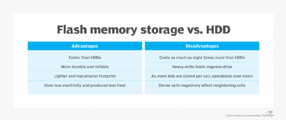
Advantages of flash memory
Ultimately, a modern enterprise expects five principal benefits from flash storage devices and systems:
- High performance. It takes time to access storage and move data between a workload and storage resources. Modern flash systems, such as the HPE 3PAR StoreServ, tout up to 3 million IOPS with latencies as low as 0.3 milliseconds. This is far faster than traditional magnetic hard drives.
- Resiliency. Modern flash storage devices are more durable than HDDs -- particularly in read operations -- because there are no moving parts and they use combinations of hardware and software to enable redundancy and facilitate transparent failover between devices in a storage array. Some flash storage systems denote up to 99.9999% availability.
- Scalability. Enterprise workloads are increasingly storage-hungry, and comprehensive flash storage systems can typically provide high levels of scalability to hundreds of terabytes or more.
- DR support. Flash is a form of storage, and flash storage systems are increasingly intelligent with support for enterprise storage features such as clustering, multisite replication, accelerated backups and restorations, and support for unexpected device failures.
- Cost-efficiency. Although flash storage can be more expensive per byte than traditional HDDs, flash storage can usually pack more storage into far less space for lower power and cooling costs. When factored in with greater workload performance, flash costs can often be about the same as a traditional HDD environment.
Disadvantages of flash memory
Despite compelling advantages, flash storage poses several potential disadvantages for the enterprise, including the following:
- High implementation costs. Flash storage remains several times more expensive than traditional HDD storage on a per-gigabyte basis. Although cost efficiencies can smooth over some of this upfront cost, businesses must still budget accordingly for flash storage deployments.
- Limited device capacity. Many flash devices, such as SSDs, offer capacities that are on par with traditional HDDs, but it's important to consider cost and performance factors before selecting specific devices or systems. Higher-capacity flash devices might be disproportionately costly; lower-capacity flash devices, on the other hand, might be relatively inexpensive but more are needed to meet storage capacity demands. Look at device efficiency and performance rather than just outright price.
- Slower writes. Flash components are designed to operate in blocks -- not bits, as with traditional RAM -- so a write operation will first erase blocks before rewriting them with new data. This takes more time and slows write operations, which could make flash undesirable for some write-heavy workloads. Flash is always faster when reading, not writing.
- Limited life. Write operations cause stress and wear on the electronic components of flash storage devices. Although modern flash devices incorporate effective technologies to extend working life, such as wear leveling and other techniques, most transistors fabricated into flash chips and devices are limited to about 10,000 write cycles. This makes flash device lifecycle management vital to any flash storage system. Flash storage might not be a suitable storage alternative for write-heavy workloads.
Hybrid flash arrays, which combine HDD and SSD storage, offer organizations the ability to harness the respective price and performance benefits of both technologies. The hybrid arrays let storage managers place frequently accessed data on speedier flash storage and house less frequently accessed data on HDDs. As a result, a data center can boost the performance of hot data while avoiding the higher cost of flash for storing cold data.
NOR vs. NAND
Flash memory is a non-volatile storage technology, which means it doesn't require power to retain data. There are two forms of flash memory: NOR and NAND. Both use floating gate transistors as the basis for memory cells that store data.
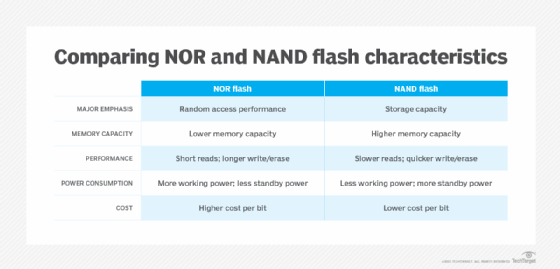
NOR flash memory was the first flash type to reach the commercial market, arriving in 1988. NOR links memory cells in parallel, emphasizing random access performance. NOR flash memory is characterized by fast data reads and slower erase and write speeds. In general, NOR technology stores executable boot code and supports applications that demand frequent random reads of small data sets.
NAND flash memory followed NOR to market about a year later. NAND is slower to read than NOR, but it takes less time to erase and write new data. NAND also offers higher storage capacity at a lower cost than NOR, so the technology's main function is data storage.
Indeed, a key objective of NAND development has been to boost chip capacity and reduce the cost per bit to make flash memory more competitive with magnetic storage devices. However, storage devices built on this technology face endurance limitations. NAND flash can support only so many program/erase (P/E) cycles, the process of erasing data before new data is written. Storage vendors use various methods to reduce P/E cycles and balance P/E loads with the goal of improving NAND flash memory durability.
Types of flash memory
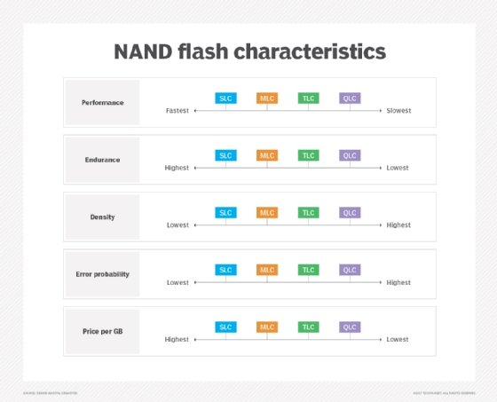
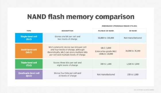
NAND flash memory is broken down into several types, which are defined by the number of bits used in each flash memory cell. NAND flash memory types include single-level cell (SLC), which stores one bit in each cell; multi-level cell (MLC), which stores two bits; triple-level cell (TLC), which stores three bits; quad-level cell (QLC), which stores four bits; and penta-level cell (PLC), which stores five bits.
Each flash memory type has its own characteristics, strengths and weaknesses, which determine how and where it's used.
SLC: Performance at a price
SLC offers the highest performance, endurance and reliability compared to other NAND types. However, those benefits come with a higher price tag. Commercial and industrial applications rank among the top use cases for SLC adoption, as organizations in those sectors are more willing to pay a premium for the advantages of this NAND flash memory type.
In general, each additional bit added to a memory cell comes with a performance, endurance and reliability penalty, all along the SLC, MLC, TLC, QLC and PLC continuum.
MLC, TLC: Cheaper, denser tools
The advantages of having additional bits in each memory cell are higher density and lower costs. MLC's price point makes it attractive to makers of consumer electronic devices, such as PCs. Enterprise MLC, however, provides more write cycles than consumer-grade MLC, making it an option for more write-intensive applications.
TLC, meanwhile, offers a still higher storage density compared to MLC but at the cost of lower performance, endurance and reliability. It also finds a niche in consumer electronics.
QLC: A fit for read-intensive workloads
Looking at QLC vs. TLC NAND as an either-or choice might be the wrong way to consider the technologies, which can prove complementary. Indeed, QLC technology's market positioning differs somewhat from TLC. QLC NAND focuses on read-intensive workloads, filling a niche between TLC flash and HDDs. The idea is that lower write endurance in more complex flash can be negated through read-intensive workloads -- where reading doesn't impose wear on flash cells.
QLC's read-intensive nature makes it suitable for enterprise applications, such as data analytics and machine learning. Other possible data center uses for QLC NAND include media streaming, where SSDs using the technology have the capacity and speed to host video files, and active archives, where data remains online and accessible.
An organization can swap out a desktop PC's aging HDD for a QLC-based SSD to significantly improve performance. Enterprises taking this approach might also be able to delay their next desktop technology refreshment cycle, avoiding undue cost -- at least temporarily -- in the process.
In general, QLC NAND flash delivers benefits at a lower cost per gigabyte, making the memory technology an affordable option compared to other flash varieties. And cost can be a key driver for organizations purchasing on an enterprise scale.
PLC: One for the archives
Finally, PLC flash offers limited endurance but low cost-per-gigabyte economy. As such, PLC targets archival applications and cool to cold data. PLC flash SSDs fall into the same class as other write once, read many technologies.
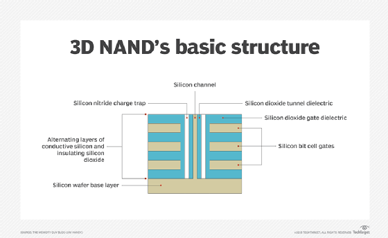
3D flash memory
The shift from planar (2D) to 3D fabrication technology is another way flash manufacturers seek to improve flash's price and capacity characteristics. 3D NAND flash stacks memory cells vertically in multiple layers. This method of layering cells dramatically increases SSD capacities and lowers the per-gigabyte cost. 3D NAND is considered suitable for any business or consumer scenario that uses planar NAND.
Higher capacity in a smaller physical space is the main advantage of 3D flash memory. Higher manufacturing cost has been the primary drawback, but the technology's price has been dropping.
Another aspect of 3D NAND is charge trap technology. Many 3D flash drive manufacturers use the charge trap approach, which provides higher endurance rates -- thus more write/erase cycles -- than flash devices with floating gate cells. Charge trap technology also supports faster read/write operations and lowers energy use.
3D flash is known by several trade names, including the 3D NAND name first announced by Toshiba in 2007, as well as V-NAND, which was first released by Samsung in 2013. Both product families employ the same fundamental operating principles.
Flash memory standards
Flash memory standards go beyond the primary groupings of SLC, MLC, TLC and their successors. Internal and external connectivity standards are also worth noting, as the typical linkup approaches are beginning to shift.
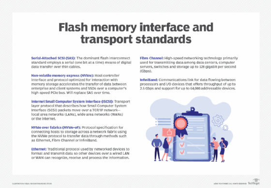
Flash standards typically relate to interface and connectivity, and common standards today include both internal and external interfaces that include the following:
- Serial-Attached SCSI (SAS). This internal interface standard is commonplace for peripheral devices, such as disk drives, but provides a convenient interface for flash components assembled into an SSD device.
- Non-volatile memory express (NVMe). This internal interface provides optimized support for flash components that communicate through the PCIe bus or new connectors, such as M.2 or U.2. NVMe provides low-latency, high-speed communication that's edging out SAS for flash-based devices.
- Internet SCSI (iSCSI). ISCSI is an Ethernet-based external interface that's robust and versatile for moving data from flash storage devices over major local and wide area networks.
- NVMe over fabrics (NVMe-oF). NVMe-oF is a fabric-based external interface designed to reduce latency and enhance flash storage communication over either Fibre Channel or Ethernet network fabrics. This new interface approach is supplanting iSCSI for flash device connectivity.
These interface standards are typically encountered when connecting flash storage devices to computer systems. In addition, flash devices typically offer some level of compatibility with broader network types, including Ethernet, Fibre Channel and, in some cases, InfiniBand.
What to consider when buying flash memory
Flash storage is now a well-recognized resource for many enterprise workloads, but the choice of flash storage is never a given. Before making any storage investment, business and IT leaders must consider the following fundamental business issues, among others:
- Use case, which includes the workload or application that the storage is intended to support.
- Data access needs of the workload or application, such as IOPS and read/write demands.
- Requirements for capacity, security and data management.
- Current storage resources.
Only then can an organization make cogent decisions about flash and its role in the existing storage architecture -- for instance, how it plays into varied storage performance tiers. When a business elects to adopt flash storage, common decisions can include the following:
- Flash capacity and IOPS performance needs.
- Form factor, such as a PCIe card for inclusion in a computer, or a standardized SSD form factor for insertion in a storage subsystem.
- Support for data and flash device management.
Select flash with care
When it's finally time to drill down into the details of flash storage options, buyers have a few particulars to weigh. One such consideration: SSD form factors. Early in the evolution of enterprise flash, the 2.5-inch SATA form factor became popular among SSD vendors looking to ease the transition from HDDs to SSDs.
The SATA standard was created for HDD data transfer and lets organizations adopt new drives more gradually. The 2.5-inch size enabled an SSD to readily fit into a desktop drive bay.
A smaller SATA SSD form factor, dubbed mSATA for mini SATA, targets laptops, notebooks, tablets and other power-constrained devices. The M.2 form factor followed mSATA, offering an even smaller SSD form factor that delivers higher performance and greater storage capacity than mSATA drives.
SSDs can also take the form of add-in cards that plug into a computer's PCIe motherboard slot.
The market's move to NVMe-based high-performance SSD technology is another aspect of flash that storage buyers should evaluate. NVMe SSDs, which connect directly to the PCI system bus, are becoming more prevalent in the enterprise. SSDs adhering to HDD form factors and interfaces haven't taken advantage of the full potential of NAND flash.
NVMe SSDs offer an edge over SATA drives because the NVMe protocol was created for non-volatile semiconductor memory, such as NAND flash. And as NVMe grows in popularity as an interconnect for flash disks and arrays, NVMe-oF products have begun to provide a workable option for NVMe-based shared storage. The NVMe-oF technology ecosystem is in a state of flux, but resources such as the University of New Hampshire InterOperability Laboratory can help evaluators identify standards-compliant products.
Vendors and products
NAND flash memory vendors vary in what they offer the market. Some manufacturers provide general-purpose flash storage, while other companies specialize in specific market segments. The following are some of the largest NAND flash memory manufacturers:
- Kioxia.
- Micron Technology.
- Samsung.
- SK Hynix (which acquired Intel's NAND business in 2021).
- Western Digital Corporation.
Some vendors offer a range of products covering enterprise and consumer applications. For example, Kioxia makes enterprise, client and data center SSDs, while Samsung's SSD portfolio is geared toward the enterprise and consumer markets.
As for marketing, vendors might sell flash memory products to other vendors that embed the technology in their storage offerings or sell storage devices under their own brand. Some vendors, such as Micron Technology, pursue both approaches.
The variability found in vendors' NAND flash offerings can also be seen in pricing. Although decreasing cost serves as the general rule for NAND flash pricing, the actual pattern at any given time is somewhat hard to pin down. Storage market analysts differ in their short- and long-term predictions for NAND pricing trends. Cyclical periods of shortage and oversupply cause NAND pricing to fluctuate. In addition, macroeconomic trends and global events -- such as the 2020 COVID-19 pandemic -- can affect demand for flash memory and, therefore, pricing.
The future of flash memory
The future of flash memory is pointing toward greater capacity as vendors push on with plans to boost the number of 3D NAND flash layers and increase bit densities. Manufacturers are racing to increase storage density while decreasing the cost per bit. For example, SK Hynix now produces a 300-layer chip with 1 Tb of capacity that uses TLC technology and writes at speeds of 194 MB per second. Manufacturers predict that 1,000-layer flash devices might be possible by 2030.
Another push is the broad adoption of PLC -- 5 bits per cell -- technology. Although PLC technology currently suffers from lower write endurance and performance, manufacturers are improving fabrication techniques and employing special algorithms to help offset these limitations.
Other anticipated trends include the increasing use of QLC drives in enterprise storage, at least for read-intensive workloads. This brings devices with higher density and lower cost per bit into the mainstream for enterprise flash devices.
Interface developments such as NVMe and NVMe-oF, meanwhile, will continue to push flash storage toward fully realizing its higher performance potential. The evolution of flash will also feed into other technologies, such as storage class memory (SCM). SCM represents a new storage/memory tier in the enterprise, existing between SSDs and DRAM, with the aim of supporting latency-sensitive applications.