
flash storage
What is flash storage?
Flash storage is any type of drive, repository or system that uses flash memory to write and store data for an extended period. Flash storage is common today in small computing devices, consumer devices and large business storage systems.
Flash storage is based on electrically programmable memory. As non-volatile memory, it doesn't require power to maintain the stored data. Digital information is stored on solid-state flash memory chips. The size and complexity of flash-based storage varies per device, ranging from portable USB drives, smartphones, cameras and embedded systems to enterprise-class all-flash arrays. Flash is packaged in various formats for different storage purposes and is often called solid-state storage, as it has no moving parts.
Flash storage has fast response times compared to hard drives with spinning disks, and is a good storage alternative to hard disk drives (HDDs).
How does flash storage work?
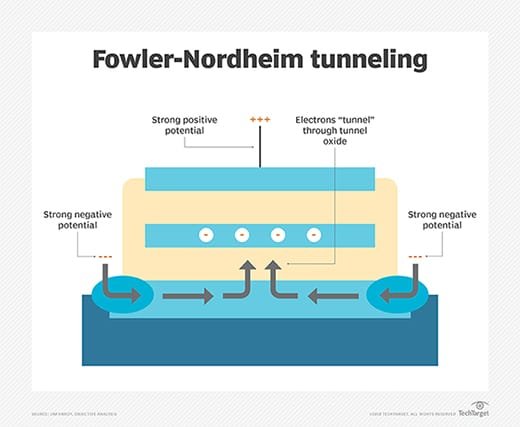
Flash stores data using a charge on a capacitor to represent a binary digit (bit). It's typically packaged in surface-mounted chips attached to a printed circuit board (PCB). Flash storage contains a grid of many columns and rows with cells that have two transistors at each intersection separated by a thin oxide layer. One transistor is called a floating gate and the other a control gate. If the floating gate is connected to the row through the control gate, the cell has a value of 1.

For the cell to have a value of 0, a barrier must be placed between the control gate and floating gate. This occurs in a process called tunneling, where excited electrons are pushed through the other side of the thin oxide layer, giving them a negative charge that acts as a barrier between the control and floating gates. Some flash chips might have millions or billions of these tiny transistors and use a logic controller, enabling them to work together.
With no moving mechanical parts involved, power consumption is lower. A typical Serial Advanced Technology Attachment (SATA) flash drive consumes 50% or less of the power mechanical SATA HDDs require and can provide sequential read speeds up to 6 gigabits per second (Gbps) in drives using SATA 3.2. With no mechanical limitation for file access, flash drive access times are in microseconds, rather than the millisecond seek times mechanical HDDs require. This lowers latency by several orders of magnitude.
Most flash storage systems are composed of memory chips and a flash controller. The memory chips store data while the controller manages access to the storage space on the memory unit. The flash controller is often multichannel, working with a RAM cache. The cache buffers the data going to and from several chips, boosting speed.
Examples of flash storage in use
Flash memory is widely used for consumer devices, including the following:
- Smartphones.
- Notebook computers.
- Digital cameras.
- Tablets.
- Gaming consoles.
- Computer BIOS chips.
- USB memory sticks and Secure Digital (SD) cards.
Flash storage adoption in enterprise storage systems encompasses the following:
- Databases.
- Virtual desktop infrastructures.
- Enterprise workloads.
- Mission-critical applications.
- Redundant arrays of independent disks (RAID) using solid-state drives (SSDs).
The history of flash storage
Dr. Fujio Masuoka is credited with inventing NOR and NAND, the two main types of flash memory, while he worked at Toshiba in the 1980s. Masuoka presented NOR flash in 1984 and NAND in 1987. Much faster than the electrically erasable programmable read-only memory (EEPROM) process, the new format's ability to be programmed and erased in large blocks reminded a colleague of Masuoka's of a camera flash.

Intel's interest was piqued because NOR flash could serve as a higher-functioning replacement for the EEPROM chips the company was shipping at that time. Intel released the first NOR flash chips in 1988. Toshiba followed with the first NAND flash chips in 1989.
The USB flash drive emerged in 2000 for file storage and transfer. It was more compact and had more capacity than earlier systems. By the mid-2000s, it looked like NAND flash would hit a hard scaling limit. The photolithography processes used to shrink transistors would no longer suffice to continue the price declines and performance improvements the industry and its customers had become accustomed to. In 2006, Toshiba developed a new process called Bit Cost Scaling (BiCS) to overcome these issues; in 2007, Toshiba announced a new flash technology, 3D NAND.
Instead of continuing to try to shrink transistors, BiCS let manufacturers greatly increase the number of transistors on a chip by building them vertically rather than horizontally, as is done with standard planar NAND technology. 3D NAND is backward-compatible with planar NAND, so any devices that support the latter can read and write data to the former and vice versa.
In 2009, Toshiba introduced three-level memory cells that could store 3 bits per cell, and soon after, Samsung introduced triple-level cell (TLC) NAND. In that same year, Toshiba and SanDisk introduced quad-level cell (QLC) NAND flash memory chips that could store 4 bits per cell and had a 64 Gbit capacity.
In 2011, the non-volatile memory express (NVMe) specification was published, with the first commercially available NVMe chips released in 2012.
In 2016, the NVMe over Fabrics (NVMe-oF) 1.0 specification was ratified and multiple vendors began demonstrating NVME-oF systems. That same year, Western Digital acquired SanDisk.
In October 2020, Intel announced it was selling its SSD and NAND business to SK Hynix for $7 billion. Until the transaction's final closing, predicted to be around March 2025, Intel continues to manufacture and design NAND flash memory. Until this time, Intel is winding down its production of Optane memory chips, but it still retains NAND-related business assets such as design and manufacturing intellectual property.
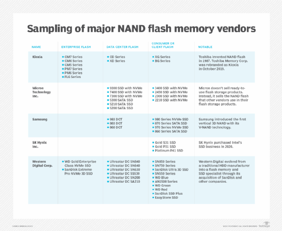
Major manufacturers of NAND flash memory chips include Kioxia America, formerly Toshiba Memory Corp.; Micron Technology; Samsung; SK Hynix; and SanDisk, which is now owned by Western Digital. Major manufacturers of NOR flash memory include Cypress Semiconductor, now part of Infineon Technologies; Macronix; Microchip Technology; Micron Technology and Winbond Electronics.
How flash storage compares to SSD
A non-volatile SSD uses solid-state flash memory to persistently store data. Its main components include NAND flash memory chips and a flash controller. The SSD controller is designed and optimized to provide high read/write performance for both random and sequential data requests. Manufacturers achieve varying densities and capacities in SSDs by stacking chips in a grid.
Although the terms flash storage and SSD might be used interchangeably, they have different meanings. SSD refers to a hard disk that contains flash storage. In other words, flash storage is just one of the components that make up an SSD. Besides flash storage, SSDs contain an interface that supports plugging the SSD into a PC's storage controller. For example, an SSD might contain a SATA interface.
All SSDs contain flash storage, but not all flash storage is used in SSDs. Flash storage is used in countless other applications such as USB flash drives, micro SD cards and smartphones.
Flash storage vs. traditional HDDs
NAND flash storage offers advantages over traditional HDDs. HDDs carry a lower cost per stored data bit, but flash drives can provide significantly higher performance, lower latency and reduced power consumption. Their compact size also makes flash suitable for small consumer devices.
In enterprise systems, flash can help a business consolidate storage and lower the total cost of ownership. Fewer SSDs are needed to process transactions and match the performance of systems using slower HDDs. Enterprises can accrue savings on rack space, systems management, maintenance, and power and cooling costs. Data reduction technologies, such as inline deduplication and compression in all-flash storage systems, also let businesses shrink their data footprints.
As interest in flash storage has grown, industry watchers have noted a frequently overlooked limitation of flash, which is that longevity might be reduced in heavy use with high write workloads. Flash has relatively limited tolerance for write-erase cycles. Manufacturers use features such as wear leveling and dynamic random access memory (DRAM) or non-volatile RAM caching to improve reliability and performance.
Unlike HDDs, which are constrained by their movable parts, SSDs come in several form factors. They are available at multiple heights with support for SATA, Serial-Attached SCSI (SAS) and NVMe protocols. The 2.5-inch SSD is the most common type of SSD. Fitting into the same SAS and SATA slots in a server, it falls into the traditional HDD form factor type of SSD, as identified by the Storage Networking Industry Association's Solid State Storage Initiative.
Other major types of SSDs include solid-state cards and solid-state modules. The former comes as a standard add-in card -- like those that, for example, use a Peripheral Component Interconnect Express (PCIe) serial port card on a PCB and bypass host bus adapters to speed up storage performance. A U.2 SSD is an example. The latter type of SSD, also known as non-volatile dual inline memory module (NVDIMM) cards, uses a dual inline memory module (DIMM) or small outline DIMM (SO-DIMM) format.
Flash storage formats
Flash storage comes in the following formats:
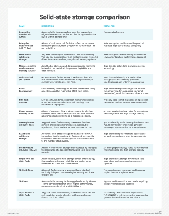
NAND flash
NAND flash memory is a type of non-volatile storage technology. An important goal of NAND flash development has been to reduce the cost per bit and increase maximum chip capacity so flash memory can compete with magnetic storage devices such as hard disks. NAND flash has found a market in devices to which large files are frequently uploaded and replaced.
Types of NAND flash include the following:
- SLC, or single-level cell, stores 1 bit per cell.
- MLC, or multi-level cell, stores 2 bits per cell.
- EMLC, or enterprise MLC, stores 2 bits per cell.
- TLC stores 3 bits per cell.
- QLC stores 4 bits per cell.
- 3D NAND, or vertical NAND, stacks cells on top of each other.
NOR flash
NOR flash offers memory addressing on a byte scale, enabling true, random access and good read speeds. It was this addressability that interested Intel in NOR. The technology matched the requirements for BIOS and Unified Extensible Firmware Interface (UEFI) applications. NOR flash is more expensive per gigabyte than NAND because of its larger, individual cell size. NOR also has slower write and erase times than NAND.
Both NAND and NOR use quantum tunneling of electrons to move electrons through the cell wall's dielectric insulating material. This degrades the material over time. NOR flash is erasable, making it a great replacement for EEPROM- or ROM-based firmware BIOS and UEFI chips, where addressability and read speed is a boon and rewrite durability is less troublesome.
NAND offers greater write speeds than NOR flash and a lower cost per gigabyte. The lower cost reflects the NAND memory cell's string design, saving die space and reducing the overall size of a chip per gigabyte. NAND can come in SLC and MLC forms, which include eMLC and TLC. SLC stores a single bit of information per cell. SLC generally offers greater speeds -- especially for writes -- greater longevity and fewer bit errors. MLC provides storage capacity for more data because its cell supports more levels of charge, which accommodates storing multiple bits of data per cell. MLC can double capacity over SLC; TLC provides a third bit. The extra levels of charge, along with smarter flash controllers and firmware, also enable bit error correction.
New Technology File System (NTFS)
NTFS is the file system for PCs running any modern Windows operating system, including Windows 10 and 11. Used for storing and retrieving files on HDDs and SSDs, NTFS has a high file size limit and is compatible with Linux.
Apple File System (APFS)
APFS is Apple's file system optimized for flash SSD storage. It replaces Apple's previous HFS+ file system for Macs. APFS-formatted drives have compatibility problems with older Macs that use HFS+.
File Allocation Table (FAT)
FAT is a file system Microsoft developed to support small disks and simple folder structures. Compatible with Windows, Mac and Linux, and found in most drives today, FAT is among the most versatile flash memory formats. However, FAT is limited to accepting individual files over 4 GB in size.
Extensible File Allocation Table (exFAT)
exFAT is a newer version of FAT with the same cross-compatibility but a much larger 16 exbibytes (EiB) file size limit.
Flash storage interfaces
The Open NAND Flash Interface Working Group develops NAND flash chip standards. NAND flash manufacturers -- including SK Hynix and Micron -- support them. These standards enable interoperability between NAND devices from different vendors.
Flash storage for computer memory comes in various interfaces, including the following:
- USB4, the newest version of USB and introduced in 2019, can transfer data at 40 Gbps between devices.
- SATA is a common format in desktops and notebook computers; the 6 Gb version can eliminate bandwidth bottlenecks. Volume shipments of 12 Gbps SAS began in 2015. SAS-based SSDs are widely used in enterprise storage systems.
- PCIe-connected flash storage provides enough bandwidth to enable future expansion and represents the extreme end of speed-demanding offerings.
- NVMe technology in use with PCIe-based SSDs further reduces latency, increases I/O operations per second and lowers power consumption by streamlining the I/O stack.
Flash in the data center
Data centers with I/O-intensive applications, such as high-transaction rate databases and credit card processing systems, are increasingly turning to flash storage as an efficient, cost-effective way to increase throughput without adding more servers.
Major storage system manufacturers offer all-flash systems and hybrid arrays equipped with SSDs and HDDs. Numerous all-flash storage specialists have surfaced to challenge incumbents. Servers equipped with flash storage are increasingly common and can further reduce latency.
Data center managers looking for ways to address the energy drain associated with HDDs are examining flash storage to achieve green computing benchmarks. Flash SSDs provide high bandwidth at much lower power consumption than HDDs, making them a good choice for this goal.
The future of the flash storage market
Initially, use cases for flash storage were limited due to its relatively high costs and tight storage capacities. However, flash storage has evolved to become much more affordable and comes with substantially larger storage densities. This has greatly increased its use and made it a method many organizations depend on.
Numerous flash storage architectures, such as 3D NAND and NVMe, continue to evolve and improve. Storage class memory, which treats non-volatile memory as DRAM and includes it in the server's memory space, has also emerged; it blurs the subtle line between memory and storage.
A growing number of storage array vendors have added support for NVMe to their products to speed up the transfer of data between flash storage and servers. NVMe exploits the high-performance PCIe bus to let applications and flash storage communicate directly.
NVDIMMs are also gaining traction. These devices, which integrate NAND flash with DRAM and a power supply, plug directly into a standard DIMM slot on a memory bus. The flash storage on NVDIMM cards is used to back up and restore data in DRAM, and the power supply is used to maintain non-volatility.
Other types of memory have cropped up as possible NAND flash replacements. Examples include the following:
- Ferroelectric memory.
- Conductive-bridging memory.
- Resistive RAM.
- Oxide-based resistive RAM.
- Nano-RAM.
These technologies aim to deliver high performance, non-volatility and low power consumption. They also promise to move the flash storage industry beyond DRAM and NAND flash scaling limits.
Learn more about the future of NAND flash, storage class memory and NVMe-oF.