New memory technologies challenge NAND flash dominance
Cost and scaling limits mean planar NAND flash as we know it will slowly cede its pre-eminent place in the memory hierarchy to emerging technologies such as 3D XPoint.
Flash memory rose to prominence as soon as Intel shipped the first NOR chips in 1988. NOR, in turn, paved the way for NAND flash three years later. NAND enjoyed the fastest adoption of any semiconductor technology ever, ramping from $1.8 billion to $18 billion in 10 short years. By 2017, the technology hit a record $50 billion in revenue, matching the size of the global semiconductor market of 1990. NAND flash is clearly big business.
But change looms as the industry develops several new memory technologies as possible replacements.
NAND flash faces hard limit
During the past 40 years, the number of transistors on a semiconductor chip doubled every year or two by reducing the size of a single bit by an average of 30% a year thanks to Moore's Law. This, in turn, drove cost reductions that enabled chips to find broader use. These 30% reductions are called process shrinks, and the ongoing phenomenon of constant size and cost reductions is known as scaling.
Continuing shrinks could be sustained for most semiconductors, but flash memory had a problem: In flash, bits are stored as electrons on a floating gate, and the number of electrons that a floating gate can hold is proportional to the size of the transistor. At the 15 nanometer (nm) process geometry, the difference between a one and a zero amounted to only a few tens of electrons, an extremely difficult number to detect amid the noise within a digital chip. If manufacturers reduced the size of the transistor by another 30%, as they have always done, the number of electrons would fall below a detectable level.
The entire semiconductor market has been built on the expectation of ongoing cost reductions. It wouldn't do for flash price declines to come to a grinding halt. But what could be done to continue to scale costs despite the hard limit faced in planar NAND scaling?
3D NAND to the rescue
Toshiba unveiled a clever solution in 2006. Rather than continue to shrink transistors built on a chip's surface, why not create a vertical structure and build transistors along the walls of the tower, similar to the vertical gardens on the walls of urban office buildings? If there isn't enough acreage on the earth's surface to plant a garden, then go and make one on the wall of your building.
Using this approach to increase the number of transistors on a chip, Toshiba planned to continue to scale the cost of a flash bit even if the transistors couldn't be scaled. It named the approach Bit Cost Scaling, or BiCS, which became the basis for 3D NAND flash.
Not only would BiCS allow cost reductions to continue, it supports continued use of NAND flash, as 3D NAND and planar NAND are similar enough to be used interchangeably with little or no redesign. A consumer may have two USB flash drives, one with 3D NAND and the other with planar NAND, and not be able to tell any difference. This is an advantage over some other new memory technologies.
3D NAND flash increases the number of transistors per chip by situating them vertically, in a manner similar to the vertical gardens on the walls of urban office buildings, like this one in Shenzhen, China.
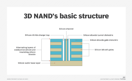
The industry adopted Toshiba's approach. With BiCS, bits are built in a column formed by filling a hole in a deep series of semiconductor layers. The question then became: How high can we build these vertical towers of bits? It's unclear.
When Toshiba first developed BiCS, prevailing wisdom figured the number of bits in the column would be limited by the number of layers in the chip and the width and depth of the hole used to create the column (see "Building 3D NAND"). Manufacturers can't make this hole smaller than about 20 nm because a few concentric layers of material must coat the insides, and those concentric layers have a minimum thickness requirement. The depth, meanwhile, is proportional to the number of vertical layers, and these layers also have a minimum thickness. Because of these restrictions, the aspect ratio of the hole -- the depth divided by the diameter -- is determined by the number of vertical layers in the flash.
Building 3D NAND
3D NAND uses a relatively simple approach to squeeze more transistors onto a chip: Build them sideways, flying in the face of the way semiconductors have always been made.
Most chips are manufactured through a photolithographic process. The patterns required to make billions of transistors on a chip are projected onto a silicon wafer's surface by shining light through something called a mask that resembles a photographic negative and then processing the unexposed parts of the silicon. This is, by nature, a planar approach; photographs are always two-dimensional.
So how do we turn this into 3D? The innovators who created 3D NAND realized certain of the highly repetitive patterns they wanted to use could be built another way. If they made numerous layers of materials on the surface of the chip, something like the cake and frosting of a layer cake, they could then etch holes through all of the layers. That would produce a structure that resembled a photograph printed sideways onto the walls of the holes. This can be done without using a photographic process thanks to the alternating layers–the pattern is already in the layers.
Of course, there's far more to it than that, but that's the basic secret of 3D NAND.
Aspect ratios of 40-to-1 are difficult to manufacture, and 60-to-1 is extraordinarily challenging. But as the layer count increases, a higher aspect ratio is required. This appeared to limit 3D NAND to three generations, or about 100 layers, before it would need to be abandoned in favor of a new technology.
Semiconductor researchers are an amazingly innovative bunch, though, and they devised a new idea called string stacking to support significantly higher layer counts. With string stacking, a certain layer-count 3D NAND is made and then another set of layers is built above it. With each new set of layers, a new hole is formed, but this hole is etched through a smaller number of layers, so its aspect ratio remains modest. For example, instead of etching one challenging hole through 64 layers, Micron Technology etches through 32 layers twice to produce its current 64-layer 3D NAND. That amounts to possibly the difference between two 30-to-1 aspect ratio holes or a single hole with a 60-to-1 aspect ratio.
Nobody knows how many times strings can stack before they reach their limit. Prevailing belief anticipates a 500-layer limit, but this is uncertain. Common wisdom is often proven wrong in the world of semiconductors.
Today's 64-layer chips come in densities as high as a terabit (128 GB), so a 500-layer chip could be expected to store almost 10 times as much data. A terabyte chip is certainly conceivable. If a terabyte chip were built on a 500-layer process it would be no larger than its 64-layer 128 GB counterpart today.
The net impact of string stacking means 3D NAND may be with us for a long time.
What about 3D XPoint?
In 2015, Intel and Micron announced a new kind of memory called 3D XPoint. This different technology promised dynamic RAM-like speeds at a price point between DRAM and NAND flash. The goal is to slip a new memory layer between DRAM main memory and NAND SSDs to improve cost/performance of computers.
3D XPoint isn't intended to replace NAND flash or DRAM, although it will likely be used to reduce the amount of DRAM required within a system to reach any given level of performance. This is a big change past new memory technologies, which were ready to replace flash or DRAM once one of those reached a scaling limit.
To date, 3D XPoint has only been made available in a PCIe nonvolatile memory express (NVMe) interface. Although NVMe is the fastest interface for SSDs, it's slow compared to the inherent speed of 3D XPoint memory. It's so slow, in fact, that although Intel and Micron profess 3D XPoint is 1,000 times faster than NAND flash, today's Intel Optane SSDs are only six to eight times as fast as their NAND flash counterparts.
Clearly a DIMM interface is necessary to unleash 3D XPoint's DRAM-like speed and take advantage of its cost/performance advantages. Intel has promised to ship 3D XPoint memory in a DIMM format, but has yet to publicaly introduce such a product. Intel revealed it has shipped these DIMMs to Google at August 2018's Flash Memory Summit, however.
Objective Analysis' 2015 report on 3D XPoint memory projected the most significant market for 3D XPoint memory would be in DIMMs for servers. We continue to stand by that finding. Today's 3D XPoint memory market is relatively tiny, consisting mainly of gamers willing to spend heavily for a marginal performance improvement (see "Intel's 3D XPoint strategy").
Intel's 3D XPoint strategy
It's to Intel's disadvantage the 3D XPoint market is so small because that prevents the company from ramping the product to high volume. Without high volume, its production cost will remain high, probably higher than that of DRAM. Yet Intel must sell 3D XPoint memory at a lower price than DRAM for it to make sense to consumers. This means Intel must lose money to establish a market.
That approach probably wouldn't add up for other companies, but for Intel the story is different. 3D XPoint memory enables the company to sell higher-priced processors, recovering the money it loses in 3D XPoint sales.
Other emerging memory technologies
3D XPoint is only one of a number of new memory technologies being researched. Some have been in development for a considerable time, such as Phase-change memory (PCM), on which Intel's Gordon Moore co-authored an article back in 1970, nearly 50 years ago.
These technologies promise high performance, low power, nonvolatility and, most importantly, the ability to move past the scaling limits of DRAM and NAND flash. But NAND flash and DRAM developers continue to find ways around obstacles that threaten to limit scaling -- 3D NAND is a great example -- postponing the possibility of newer technologies displacing NAND and DRAM.
Cost is the most important factor preventing these technologies from displacing established memories.
The embedded memory market will most likely spawn one or more of these new technologies. But it may be a long time before one of these technologies has the opportunity to displace either DRAM or NAND flash. Embedded memories will adopt a new technology sooner because the memory on a logic chip must be easy and economical to build on the logic processes used to manufacture ASICs, microcontrollers and microprocessors.
NOR flash, the most common nonvolatile memory on such chips, has difficulty scaling past 45 nm, although lab prototypes have been built using processes as small as 14 nm. Similarly, even static RAM is proving troublesome, with the size of an SRAM bit failing to scale in proportion to the process. This threatens to cause the SRAM portion of the chip to balloon and limit the cost advantages that could be realized by scaling ASICs, microcontrollers and microprocessors to a smaller process.
Both NOR and SRAM are candidates for replacement by new memory technologies. Here are a few:
Magnetic RAM (MRAM) is based upon magnetic technologies already in high-volume production for the manufacture of the heads in HDDs. Everspin Technologies has been producing this nonvolatile technology as stand-alone memory for about five years, and an embedded version is being developed at all leading foundries. MRAM is based on a DRAM-like one-transistor cell, allowing it to compete on cost against DRAM, but not NAND flash.
Phase-change memory is the basis for Intel and Micron's 3D XPoint memory. It went into production as a substitute for NOR flash about a decade ago, but it was only introduced by Intel, Samsung and STMicroelectronics, all of which have abandoned the product.
Ferroelectric RAM (FRAM) has been in production for more than 20 years, but has enjoyed limited acceptance due to its reliance on lead-based materials that undermine the integrity of the underlying silicon. Despite this Fujitsu has produced more FRAM-based chips than probably all other alternative memories combined. New research has determined a friendlier and better-understood material -- hafnium oxide -- can serve as a ferroelectric layer, renewing interest.
Conductive-bridging RAM (CBRAM) is based on the migration of metal filaments through chalcogenide glass. Adesto Technology is the only company shipping this memory type.
Resistive RAM (ReRAM) from Crossbar is sampling a somewhat similar technology, in which nanometal filaments are grown through a chalcogenide glass layer. ReRAM has developed a type of bit cell that includes an internal selector mechanism, simplifying the production process while removing the need to develop a separate selector that works with the bit cell.
Oxygen depletion RAM (OxRAM) is based on a phenomenon similar to CBRAM, where oxygen ions are removed from a chalcogenide glass to form a conductive path. The technology isn't in production. Hewlett Packard Enterprise planned to use OxRAM in its advanced computer, called The Machine, until a year ago, but its approach -- called Memristor -- was postponed until recently.
Nanotube RAM, or NRAM, by Nantero is based on a layer of carbon nanotubes that can be electrically compressed or expanded to create a high- or low-resistance state.
With the exception of MRAM, all of these technologies are based on two-terminal selectors. These selectors support a tiny bit cell size -- 4f², or four times the size of the smallest feature optically printed on the chip. They also can be stacked in a method similar to 3D XPoint memory for anticipated lower costs.
Until the recent discovery that you could use hafnium oxide to manufacture FRAM, all of the above technologies required the use of new materials not as well understood as the underlying silicon. This has stood in the way of their adoption, because these new materials could thwart moving into mass production.
Cost is the most important factor preventing these technologies from displacing established memories. All are orders of magnitude more expensive than DRAM or NAND flash, keeping them from being used in anything other than niche applications where some technical feature offsets their prohibitive cost. For FRAM, it's the technology's fast write at low power. For MRAM, it's the fast write and nonvolatility without the need for an unreliable battery. PCM has been chosen for satellites because of its high radiation tolerance and CBRAM, for similar reasons, in surgical instruments sterilized with high doses of X-rays.
Until one of these technologies reaches high enough volume production, though, none is likely to achieve the low cost needed to displace any established memory technology. They won't be produced in high volume unless there's a market, and the market won't develop until prices come down. It's a chicken-and-egg issue.
What to expect in the next decade
NAND flash is expected to remain in play for at least another decade, with DRAM following along. If Intel achieves its 3D XPoint goals, then it will ramp into high volume -- although it will probably have to sell the technology at a loss initially to get to that point. The other new memory technologies, will see success as on-chip memories in the nearer term, but likely won't compete against stand-alone DRAM and NAND flash chips for quite some time.