metal-oxide semiconductor field-effect transistor (MOSFET)
What is metal-oxide semiconductor field-effect transistor (MOSFET)?
The metal-oxide semiconductor field-effect transistor (MOSFET, pronounced MAWS-feht) is the most common type of field-effect transistor (FET). They act as electrical switches and amplifiers controlling the amount of electricity that can flow between the source and drain terminals based on the voltage applied to the gate terminal.
MOSFET is the underlying technology for most discrete transistors, digital logic, integrated circuits (IC) and thin-film transistor (TFT) LCDs. They are the workhorse in modern electronics and are considered the most manufactured item in human history.
A MOSFET consists of four terminals: the source, the drain, the gate and the base. Commonly the base is connected to the source terminal. The substrate, source and drain consist of either positive or negative doped semiconductors. The metal (or conductive silicon) gate terminal is separated from these by a nonconductive oxide layer. By applying voltage to the gate, it changes the electrical properties of the semiconductor underlying, either allowing or inhibiting the flow of electricity between the source and drain.
Several intrinsic qualities make MOSFETs the most common transistor type. They use less power and have higher switching speeds than other transistor types. They can also be easily miniaturized and packed into high densities making them perfect for integrated circuits. They also only require relatively simple manufacturing and processing.

What are MOSFETs used in?
The MOSFET is the most common type of transistor today. Their primary use is to control conductivity, or how much electricity can flow, between its source and drain terminals based on the amount of voltage applied to its gate terminal. This can be used as a switch to turn on and off another circuit or other transistors, forming the basis of digital logic. They can also be used to vary the amount of conductivity for analog circuits and act as signal amplifiers.
Power MOSFETs are used to control high current or power in circuits. These are often single transistors packaged as discrete components. These are common in switching power supplies and motor controllers.
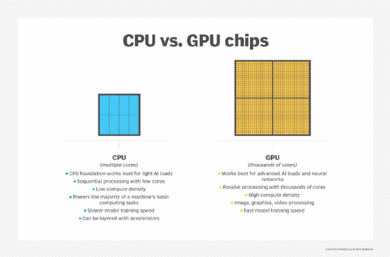
MOSFET ICs are when many MOSFETS are put on a single chip. These can range from just a hand full of transistors to a few billion individual transistors in modern CPUs and GPUs. This forms the underpinning of Moore's law. Modern high-performance MOSFETs are now only a few nanometers in size, approaching only a few angstroms in future manufacturing processes. Modern ICs use a complementary MOS (CMOS) configuration due to its better power use.

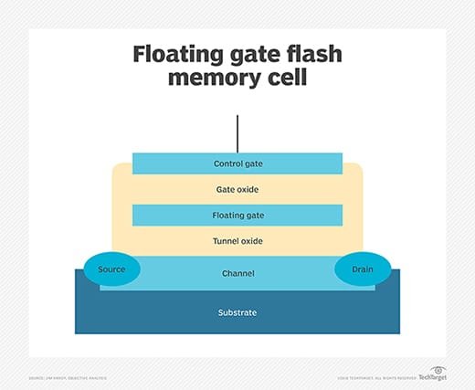
MOSFETS are also used in computer memory, both for RAM and ROM. In older SRAM the state of a transistor in a flip-flop is used to store a binary bit. Modern DRAM uses the charge of a MOS capacitor to store the data. EPROM, EEPROM and modern flash memory use floating gate MOSFETs to store data.
MOS capacitors form the basis of many sensor types. In digital imaging, the photon's charge is stored by a MOS capacitor and then read out by an IC in both older charge-coupled device (CCD) and newer CMOS active-pixel sensors (CMOS sensors). MOS technology is also used in biological and chemical sensors.
Types of MOSFETs
MOSFETS broadly fall into several categories depending on the underlying chemistry and use.
PNP and NPN MOSFETs
Pure silicon is a semiconductor and does not conduct charge on its own. By adding impurities, or doping, the silicon becomes slightly charged and capable of conducting electricity. When the doping element has an extra valence electron it becomes a negatively charged n-type conductor. Common n-type doping elements are phosphorus, arsenic and bismuth. When the doping element is missing an electron from its outer shell (only has three valence electrons) it becomes a positively charged p-type conductor where the electron holes carry the charge. Common p-type doping elements are boron, gallium and indium.
In a MOSFET the body is a lightly doped region of either p- or n-type. The source and drain terminals are highly doped regions of the opposite type of the body. This creates a "sandwich" structure of positive-negative-positive (PNP, p-channel) or negative-positive-negative (NPN, n-channel) silicon, with the gate above insulated from the silicon.

Enhancement and depletion type transistors
In an enhancement type transistor, the source and drain terminals are isolated from each other by the body. When no voltage is applied to the gate no current can flow between the source and drain. Applying voltage to the gate influences the underlying body to allow current to flow. An enhancement mode transistor can be thought of as a "normally open" switch.
In a depletion type transistor, the highly doped source and drain terminals are connected to each other by a lightly doped region of the same type. When no voltage is applied to the gate current can flow between the source and drain. Applying voltage to the gate influences the underlying body to resist the current flow. A depletion mode transistor can be thought of as a "normally closed" switch.
Both NPN and PNP can be made into enhancement or depletion mode transistors creating four basic types of transistors. This allows for the transistor to be designed to use either positive or negative controlling voltage.
Other MOSFET types
In CMOS logic, opposite (or complementary) pairs of p-channel and n-channel transistors are used together. By doing so power is only briefly used when switching between on and off states. This greatly reduces power needed and heat generated by a circuit compared to just n- or p-channel logic. Because power and heat are the greatest concerns in modern IC design, CMOS has become the dominant design for logic gates.
A MOS capacitor is a simpler device than a MOSFET. It has a similar construction to a MOSFET but lacks the source and drain. The gate and body create a small capacitor that can store an electric charge. This capacitance can be used in volatile RAM to store a bit or in a CCD to collect the charge.
In a floating-gate MOSFET (FGMOS) the gate terminal is not directly tied to a terminal. Instead, it is electrical isolated but has other secondary gates that influence it. This allows the gate to be switched from one state to the other. This is utilized in non-volatile memory such as EEPROM and flash memory to store data.
How are MOSFETs made?
Semiconductor fabrication is performed in many steps, building the transistors and circuit one layer at a time. The process typically starts with a wafer of pure silicon.
- Deposition builds a new layer upon an existing layer. This is often done in a chemical vapor deposition process.
- Photolithography shines a light through a mask to define areas of a layer. The mask defines what areas get light and defines the resulting shape of the resulting structures. The light chemically alters the masking layer protecting it from the next etching step. Due to the extremely small size of modern transistors, normal visible light wavelengths are too long, so ultraviolet (UV) and new extreme UV light is needed in this step.
- Etching uses an acid chemical to remove the topmost layer of material that is not protected by the mask.
- Washing removes any residual chemicals.
- Doping layers are where the additional elements or ions are implanted to create the p- and n-type layers.
Completed chips are then cut, tested and packaged. In packaging the silicon chip is put into a plastic or metal case that contains the contacts needed for the resulting chip to interface with external components. These packages can be in various forms such as through-hole packages, dual in-line package (DIP), thin small-outline package (TSOP), pin grid array (PGA), ball grid array (BGA) or land grid array (LGA).
MOSFET history
Early transistors were often bipolar junction transistors (BJTs). These were relatively large and difficult to mass produce and miniaturize. The principles of the field-effect transistor were theorized in the 1930s and 1940s, but no practical devices were built. In the 1950s the ability to grow an insulating silicon-oxide layer on semiconducting silicon was shown.
The invention of the MOSFET is credited to Mohamed Atalla and Dawon Kahng when they successfully fabricated the first working sample at Bell Labs in November 1959. From the 1960s onward the MOSFET quickly grew in popularity, replacing older technologies such as vacuum tubes and BJTs.
It paved the way for integrated circuits and the modern information age and is considered the most manufactured item in human history with billions being produced on each modern CPU.
See also: Flash memory guide to architecture, types and products and cache vs. RAM: differences between the two memory types.
